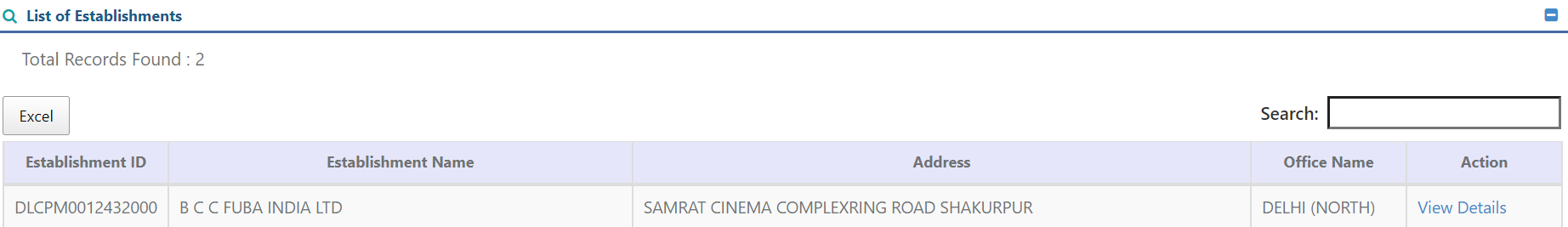
B C C Fuba India Ltd: PCB Manufacturing Nanocap

About the company:

Set up in 1985 for the manufacture of professional-grade PCBs, BCC Fuba India Limited was one of the early entrants in the Indian PCB market. It took root as a joint-venture collaboration with Fuba Hans Kolbe & Co., Germany, a company having the fine distinction of being the largest PCB manufacturer in Europe, along with DEG, Germany, a well-known European financial institution. Accordingly, the facility was set up and developed with the most high-tech machinery imported from Germany, Italy, France, the UK and the USA. Further, the company was infused with a powerful impetus package that combines the world’s best technological inputs with the complete manufacturing and quality control processes and skills, including certain special methods innovated and known only to Fuba Hans Kolbe& Co to date. To this, we have constantly made advancements keeping in mind the change in technology and the needs of our customers.

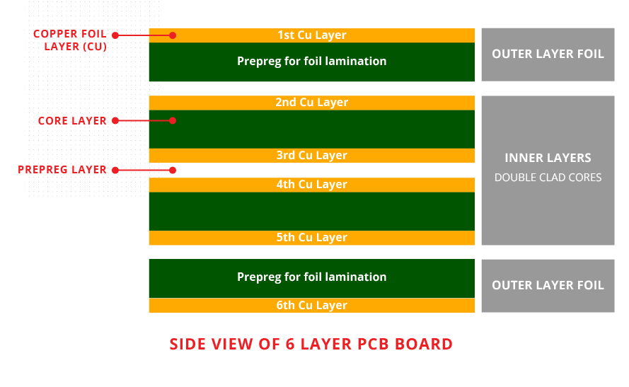
The Company is in the business of manufacturing single-sided, double-sided and multilayer (up to 8 layers) PCBs for a vast variety of applications.

Today, with our combination of highly advanced equipment and an expert, experienced team, we bring only the highest quality standards to the table. Our long list of eminent clients pays testimony to this.

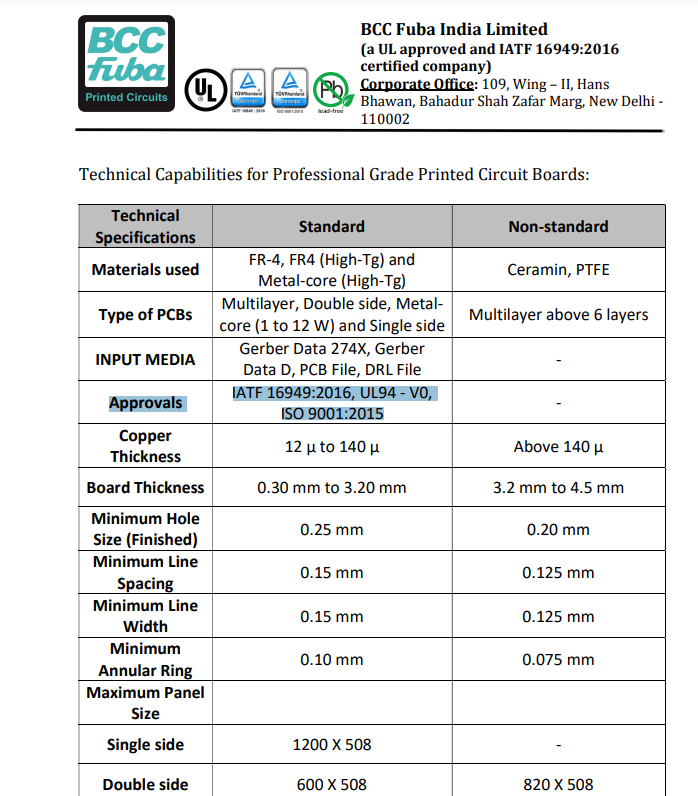
Over the years, we have been awarded the IATF 16949:2016 certification, along with the certification by the Underwriters Laboratories (UL), USA. We are, therefore, certified to meet all DIN and US MIL standards and IPC specifications.

Facility Location:

Our facility is located in the clean environment of Nalagarh, Himachal Pradesh, situated at the foothills of the Himalayas. The facility was designed and constructed under expert guidance from Fuba Hans Kolbe Germany and is fully air-conditioned and dust free.

Built on around 5 acres, the facility is geared to meet all the requirements of PCB manufacturing, especially when it comes to utilities. The facility also has ample unused space for future expansion.

Point of Change (New Management):

The year 2016 marked the dawn of a new era along with the entrance of the new promoters of the company, having existing business interests ranging from cable manufacturing, AC coils manufacturing, and manufacturing and distribution of goods like switch gears, LED lights and switches. The group has its manufacturing facilities situated in the hill state of Uttrakhand, Haryana, Rajasthan and Karnataka.

30-year-old, Abhinav Bharadwaj has been appointed as the new CEO from 1st Aug, 2023. He is also a CA.

Products:

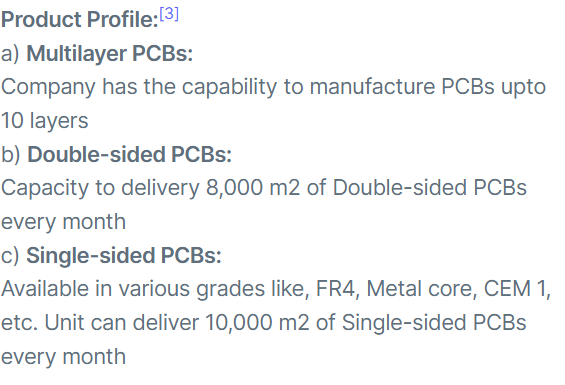
  1. Multilayer PCBs: As electronic equipment becomes more complex and compact, the precise miniaturisation of devices becomes very critical. BCC Fuba has been manufacturing and exporting multilayer PCBs since its inception and has the capability to manufacture PCBs up to 10 layers.
  2. Double-sided PCBs: Set up in 1989 along with Fuba Germany, our Double-sided PCB manufacturing unit has the capacity to deliver 8,000 m2 of Double-sided PCBs every month.
  3. Single-sided PCBs: Our state-of-the-art Single-sided manufacturing unit has been set up recently which can deliver 10,000 m2 of Single-sided PCBs every month. We can offer Single-sided PCBs in various grades like FR4, Metal-core, CEM1, etc.

Shift in Business from Trading to PCB Manufacturing:

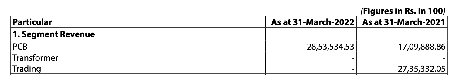
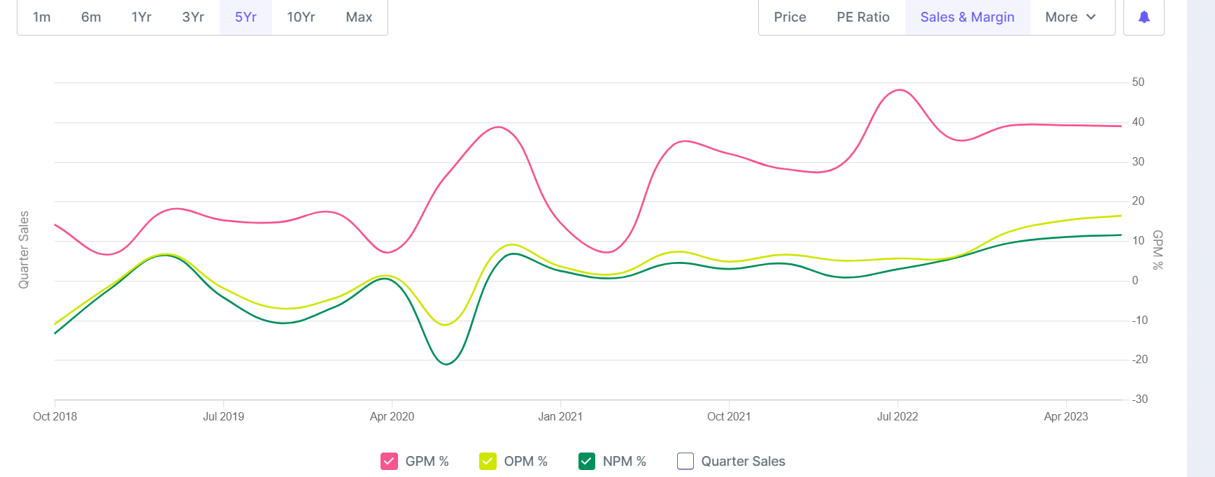
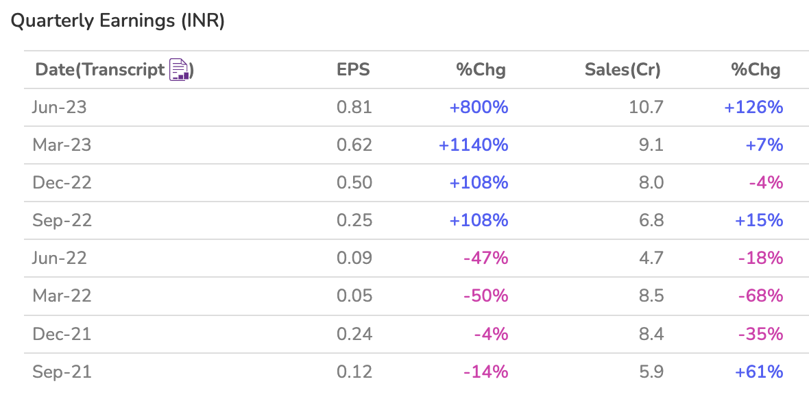
Acceleration in Net Profit YOY:

PCB Manufacturing Industry in India:

Does the company have any technical edge?

As per the concall notes from Keynes Technology in Aug 2023:

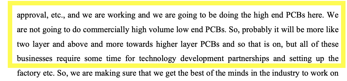
Two-layer and more PCBs are more technologically superior and are a high-margin business. It takes time for technology development partnerships. The company already has the tech to manufacture 8-10 layer PCBs.

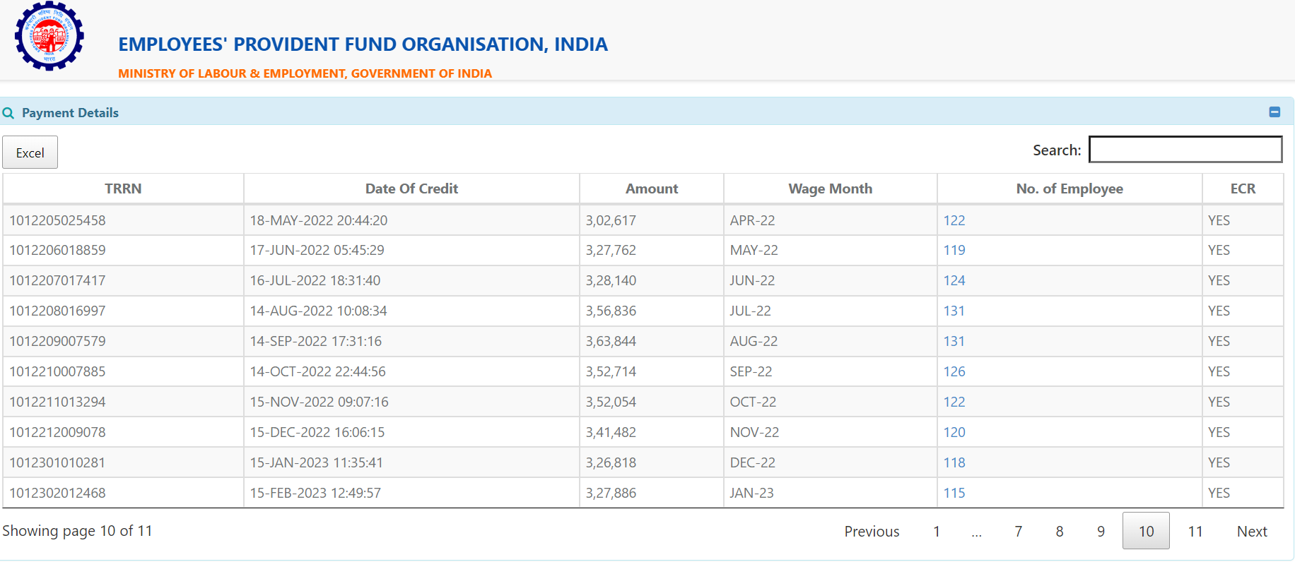
Company is doing New Hiring:

About the Technology Partner Fuba Printed Circuits:

Established in 1991, Fuba Printed Circuits is one of the leading providers of printed circuit board services from product concept to maturity.

Fuba is focusing on high-quality multilayer PCB mass manufacturing for the European automotive industry, as well as the U.S.A. Making use of a lower cost base in Tunisia, FUBA has established long-term supplier relations to serve the demands of well-known automotive first-tiers and OEMs…

Its 22 years of experience in PCB manufacturing across a myriad of customers enables Fuba Tunisie to cater to the specific and technology-driven challenges from the automotive, medical, telecom and industrial sectors. Fuba Tunisie has always prided itself to be the one to offer advanced copper inlays, controlled depth, impedance control and up to 26 layers of technology.

FUBAs strategic plan is focusing on expanding into high-tech, high-reliability PCB manufacturing in larger serial production.

Risks:

  1. 65% of the Raw materials/ chemicals/ stores and spares are imported.
  2. Non-technical promoters and management
  3. Need to see the direction of related party transactions
  4. Limited information about the company
  5. Low liquidity in nano cap
  6. Fuba Printed Circuits has reduced their stake from 8.79 to 3.48

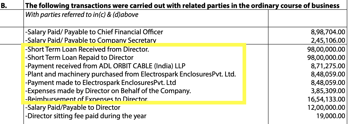
Related party Transactions in FY 2021-22:
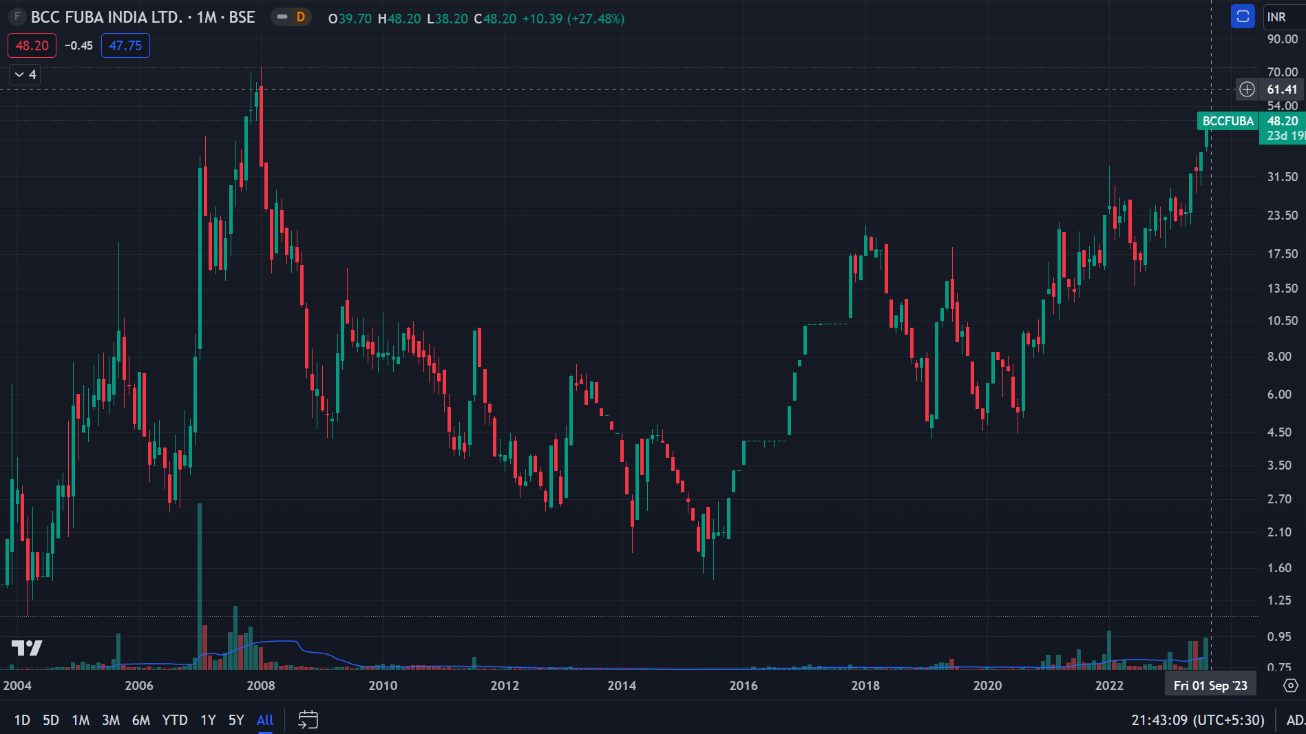
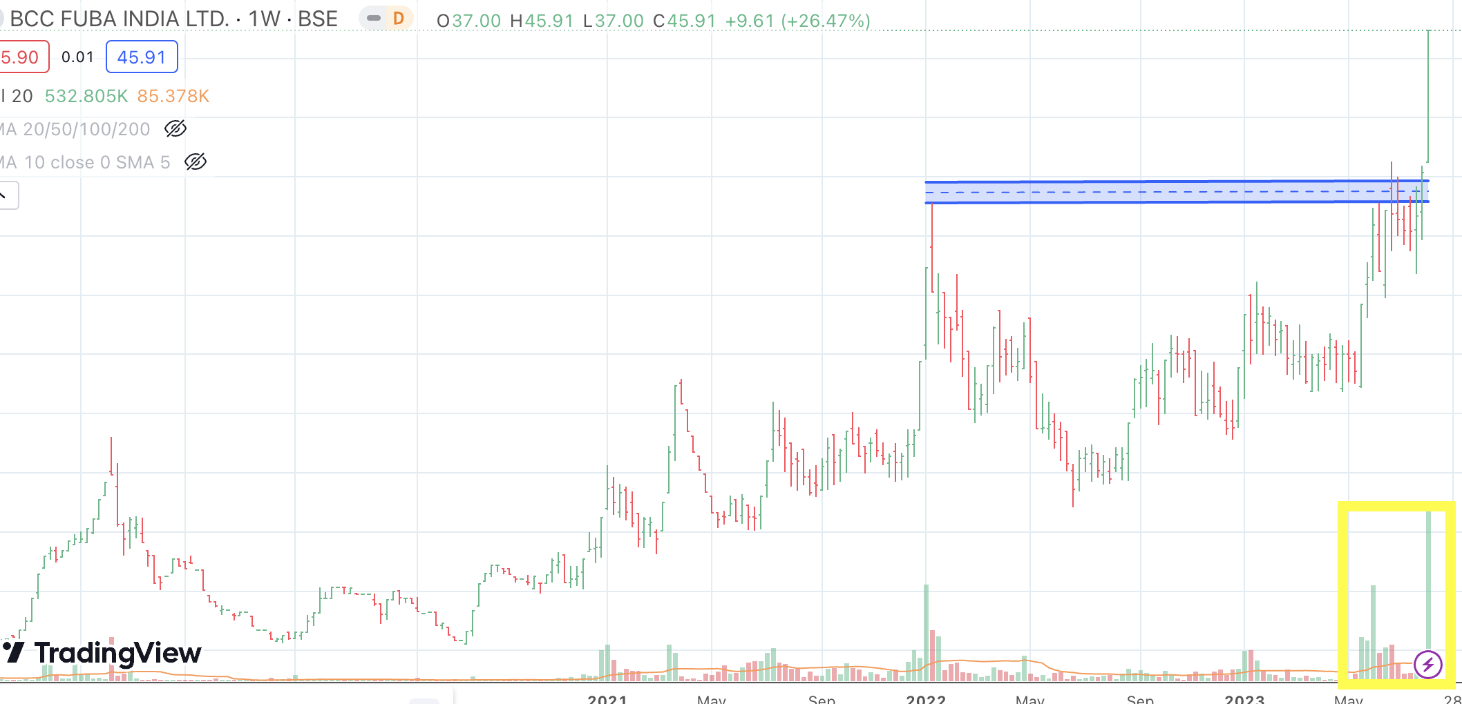
Technical Charts:

Breakout on huge volumes

Investment Rationale:

  1. Company is not even in the top 10 PCB manufacturers in India.
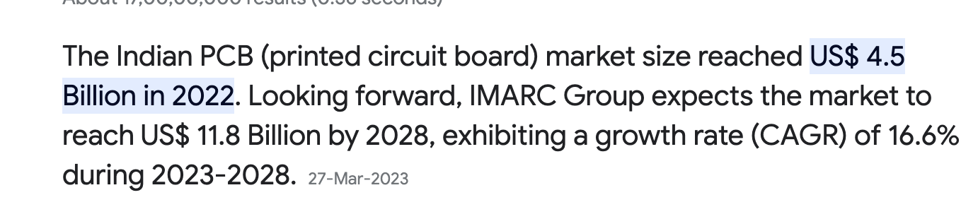
  2. PCB market is valued at 4.5 Billion$ in 2022 and is continuously growing.
  3. PCB market will grow even further in the rising electronics industry in India.
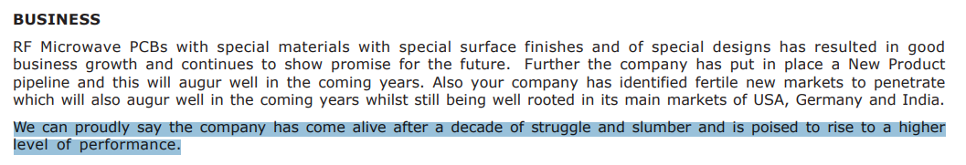
  4. Change in management has given a fresh impetus to the company.
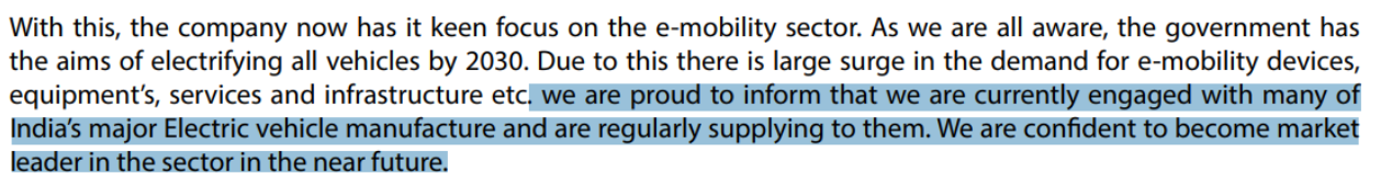
  5. Company already has the tech and is in partnership with the German company.

Open questions:

  1. Does Fuba Printed Circuits GMBH is an exclusive technology partnership with the company?
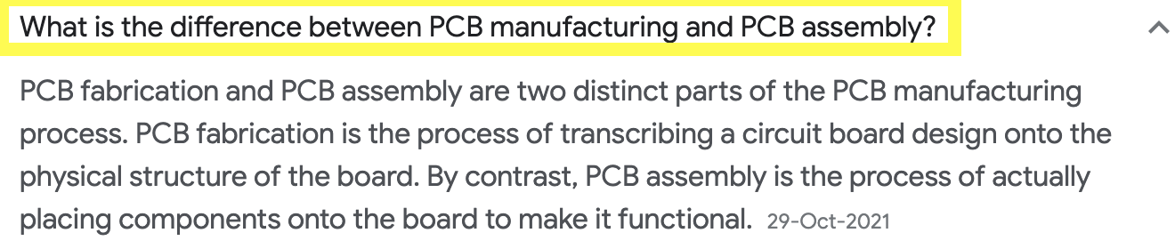
  2. Is the company doing PCB manufacturing or PCB assembly? (Just need confirmation)
  3. If they had such good technology why the company was not able to scale in past?

Please share your valuable findings if you have researched the company.

Disclosure: Currently evaluating the company.

Current Market Cap: 70 cr.
Price: 45.9

18 Likes

Thanks for summary @avneesh , have done some cursory research post Q1 results, AR 22 has some interesting pointers, this year AR and AGM should thro more light.

  • Co seem to be focused on some segments - key focus area - snapshot from AR 22

  • Margin trajectory is healthy post new promoters taking charge - GMs have expanded and trend seems healthy

  • One can do google to understand realization difference between single layer vs double sided - comes to 3X range approx - indicates value addition (also validated in above post per Kayne notes)

here are current capacities - based on broad realization trends - company is making healthy margins at modest utilization (60% type broadly by very high level calcs ) - This is something that need more work as product mix may change margins a lot
image

  • One thing that stood out for me was UL certification & IATF certification(key for auto industry usage and aligns with mgmt AR call out above) - now this may be based on Fuba global exposure and association - it could be a key asset/differentiator if co truly exploits it well going ahead

  • Some info on product range

  • In some ways company potential ties to ESM rise + make in india push fortunes - explains good show in recent past vs longer history of no performance delivery, New promoter likely deserves some credit too.

  • On quick research it appears that many unlisted players are manufacturing PCB in india (YT has some videos) - however it is likely that broadly there will be min two categories - 1) mission critical apps - medical / auto/defense etc vs 2) consumer electronics/toys etc. Category 1) is where UL type certification+ sophisticated mfg infra + skills and complex products (double or multi layer) will come into play and serious players will choose this path.

  • PCB assembly is commodity and almost everyone seem to be doing it.

  • New promoters are increasing stake(Bharadwaj family), Old hands are exiting(past promoter + others) - explains large volumes and bulk deals - absorption by mkt says accumulation as well.

  • Copper clad plates etc as RM imports context (price + freight) seem to be helping now co (after playing reverse role in last year) - However margins pressure in FY 21/H1 FY 22 indicates pricing power may not be present and this needs validation.

There is lot to understand about company, however being a nano cap information may be tricky. Current phase of bull mkt makes it even more tricky where everything is roaring :slight_smile: . If this story does play out as Electronic mfg proxy with some tech edge, should have a decent long runway and hopefully enough opportunities to ride.

D - Hv small positions post Q1 nos, most of above are feelers/quick research data and could be off, pl apply own discretion.

19 Likes

Most probably they are manufacturing as they have mentioned on their website that “They use approximately 2,00,000 liters of water every day in their manufacturing process.”

Such an amount of water is used during the “Plated Through Hole(PTH) and Etch Layer” process during manufacturing.

12 Likes

@Dev_S - Basically there are two kinds of PCBs

  1. Single Layer
  2. Multi-Layer

It will be easier to understand the “layer” once you understand the types of electronic components. There are broadly two:

  1. Through Hole
  2. Surface Mount Technology

Through Hole v/s Surface Mount: Every electronic that goes on the board usually has legs. A leg is the shiny silvery part of the component where the soldering is done. For example: in the image below, you can see 4 or 8 thin silver strips.

The above image is for through-hole components. They get the name because the board has to be drilled to make a hole so that their legs can be put across the board and soldered on the other side. For example: in the image below you can see how the component has occupied two sides of the board (on the leg-side, soldering will be done).

The surface mount components are the ones where “no hole” is needed to be drilled. Rather, the components just sit on the same side as the circuit (in the image below you can see that the legs are soldered on the same side as the component’s head).

Importance of SMT: There is no need to drill holes. You can have two separate circuits (or even more) on the same PCB. Further, as of today, SMT components are much smaller in size as compared to through-hole components which means we can have smaller devices. How much size reduction are we talking about? I doubt that we could ever have a pocket-sized smartphone if it has to be built with through-hole components. There are other differences but for this post’s sake, I’ll keep it here only.

So now, let’s understand a layer. A layer is the side of the PCB which contains the circuit (the shiny silvery path) and the components.

So, what is a multi-layer PCB? Imagine a PCB with xyz components. Now you stack another PCB on top of it. This is adding a layer. Now for the exact definition, a multi-layer PCB is basically a single board that has multiple layers of circuits and components. As a viewer, you may not be able to see all the layers as it’s usually inside the board while you can only see the inner and the outer layers

Modern systems usually have multi-layered PCBs. Through hole still exists but majorly where a cost reduction or low-end system is needed (the cost parameter can be debatable). Apart from our TV remotes (if old) and inverters (if old), I can’t think of a device that is available in our homes and is made only with through-hole components or has a single-layer PCB only :thinking:.
It would be very difficult to fit a complex through-hole-based system in the limited space of an automobile - not unless the OEM is happy to serve a low-end bulky product to the end-user (Definitely not in a system as Tesla would have)

Source: I used to work as an engineer in an electronics system-making company. Have designed systems for a pilot project of H_L’s Pure-It, Chai P_int’s Coffee machine, ZoomC_ar’s vehicles. We would design our circuits in India and get the multi-layer PCBs imported from China. Doing it in India was unsustainably costly - if needed, SMT assembly was done inhouse (which BCC Fuba seems to be doing for its clients).

35 Likes

We would design our circuits in India and get the multi-layer PCBs imported from China. Doing it in India was unsustainably costly - if needed, SMT assembly was done in-house (which BCC Fuba seems to be doing for its clients).

So, you feel that BCC Fuba is doing SMT assembly not PCB manufacturing. You already have experience with SMT assembly in the past as you have done it in-house. I had a few questions so we can narrow down what the company is actually doing.

  1. You would get PCB boards from China and paste the components (resistors, ICs, etc.) on that board (hope, that’s what SMT assembly means). Was it done manually or via machines?
  2. Is there any need for a technical partnership for SMT assembly?
  3. I guess there would be hardly any value addition for pasting components on a board. Instead, I feel BCC Fuba might be manufacturing these PCB boards. Or is this not possible in India and we need a fab to manufacture these boards?

I have low technical expertise in this field. It would be a great help if you can share your understanding.

Not exactly.

I am not saying that they are NOT fabricating PCBs. I am saying that they could be assembling whereas when fabrication of the circuitry is concerned → I do not have enough data to be fully convinced that they are manufacturing complex PCBs (end-to-end) → unsurety doesn’t mean denial

I’ll explain my rationale and let you judge before sharing my detailed POV. To keep things simple, here’s how I will divide the PCB manufacturing steps:

  • Green is where I think they might have the skills/manpower
  • Yellow is where I am unsure they have skills/resources (once again, unsurety doesn’t mean denial)
  • Red is where I can’t find an employee at BCC

Now I’ll try to showcase, why I think the probability of them doing end-to-end PCB manufacturing is low.

I have taken the below employee details from their AR of FY22 (on LinkedIn, they seem to have even fewer employees - 3).

In the best case, they have a maximum of 5 technical employees to do everything.

  • Sr.Engg, Asstt Engg & HOD Quality: Looking at their skillsets I guess they are involved in Step 1 while QA is Step 5.
  • Production Officers: I am not sure how to consider Mr.Sharma - but since this is the best-case scenario, let’s assume production officers can do everything else than step 1.
  • Manager (Maintainance): I assume this person is at max involved in steps 5 and 6 - unless “maintenance manager” refers to the person who is responsible for taking care of the office such as cleaning/opening of the premises etc.

We haven’t even considered the worst-case scenarios (if I consider worst-case, would the probability be in favor of investors?). I’ll leave you with some open questions (I do not have definite answers here):

  • Who would the run PCB fabrication machinery?
    – Are the engineers running it?
    – Can a team of 2 production officers run the PCB manufacturing machinery?

Being a little daring, I’ll put up some more questions:

  • If PCB manufacturing is this easy, then why would companies outsource PCB manufacturing?
  • Let’s say it is this easy. PCBs can be manufactured by buying machinery and a two-person team. Then is there a moat for you to invest in?

My POV:

  • What piece in value chain does BCC fit in: Locally-made electric rickshaws also have a PCB. Automobile machinery such as wheel-balancing machines have a PCB (a friend of my father used to manufacture those machines in India back in 2015 and his PCBs were made in India). However, the system is very far from what you would expect in a commercial passenger electric vehicle such as those in a Tesla (or Ather’s bikes might have). Maybe BCC is manufacturing PCBs for lesser complex systems. Maybe it’s just a small module such as a lighting system :thinking:

  • Team fails to convince me: Making reliable PCBs is more than just cost. From designing a circuit to shipping it, the entire stage is complex (for example: choosing the right component before designing itself is challenging, then while packaging certain PCBs cannot be touched with bare hands as it can damage the PCB). I am not 100% convinced that all of this can be done with the given 5 technical members. I think the probability is against me.

  • But maybe I am wrong: They have quantified the water they need as a part of the production. So maybe I am wrong and being judgemental. They could be using their employees more efficiently than I am thinking. I haven’t spent much time researching them so please don’t blindly go by my words. I would love to be wrong here because I want to see multi-layer PCBs being manufactured and exported from India someday.


  1. You would get PCB boards from China and paste the components (resistors, ICs, etc.) on that board (hope, that’s what SMT assembly means). Was it done manually or via machines?
  2. Is there any need for a technical partnership for SMT assembly?
  3. I guess there would be hardly any value addition for pasting components on a board. Instead, I feel BCC Fuba might be manufacturing these PCB boards. Or is this not possible in India and we need a fab to manufacture these boards?
  1. No and Yes.
    So the entire system is divided into modules. Let’s say you have a modern car. It will likely have multiple modules such as a lightning module that maintains the headlights, GPS tracking system etc. All of these modules will together form the system. At times we would get the components assembled from China (Machines do the assembling). At times for certain modules, we will do it in-house from hand. Another scenario is when suddenly some component change is needed in a module that was made in China, we would do it with hands. However, for large commercial production, soldering is preferred with machines.

  2. I am sorry but I do not have an answer here. My experience says large-scale professional SMT assembly needs proper investments and machinery. If manual soldering is concerned, at times, it is not humanely possible to solder components manually.

  3. PCB manufacturing is already done in India - but it depends on the complexity of the system you are thinking of. A smartphone’s PCB will be different than TV remote’s PCB. The central system of an autonomous electrical vehicle will be different than headlight module of a scooter.

I have worked in designing and programming electronic systems and not in the “fabrication of PCBs”. There are a few details that I am not aware of and this is where I will recommend that you do more research.

(There are a few things I would like to add especially about the “copper clad” mentioned in their AR. I haven’t been able to add the details due to time crunch. Will try to them add later)

Disclaimer: I have no position on this stock. I do not have plans to own this stock unless I am convinced and foresee them scaling big.

15 Likes

Some additional data points

Employee base

There are some external sources to validate what mgmt is saying vs external facts, peers/industry info

AR 22

EPFO website - seem to corroborate

Skills - there is a JD of open position on co’s linkedin site - look at the folks who have shown interest in opening and pedigree of current organizations they work for. Some merit in argument that they know where they are betting as a future employer being in same industry.

Industry / peers commentary
Fine line circuits looks like a peer with similar capabilities - we can see what they are saying in their last AR etc (funny enuff hitting UCs without number delivery yet, rub off of Fuba BCC results or a bull mkt :slight_smile:)

what are charts saying - it could be interesting if they were to take out there previous all time high seen in 200-8 time frame

At the end of day this is a nanocap stock, probably highest risk category, Ask yourself - if it was a well discovered name with possibly clear answers to all questions on past present and future - will it be available at these valuation? requires one to know self, risk appetite, if taking a plunge then risk management and so on…

while capability evaluation & validation can be evolving/perpetual exercise - as investor we should be able to take a risk reward view, else move on as bull mkt is full of ideas :grinning:

D - same as before and could be completely wrong in assumptions/cursory research done, apply own discretion

5 Likes

Also, few more points to consider is - their partnership with Fuba and DEG. Fuba is a global major with over 3 Bn marketcap and over 1 Bn revenues, with multiple patents to its name. That gives some credibility to the company. Otherwise, Why would such a big company partner with a nanocap?

3 Likes

Pursuant to section 96 of the Act and Regulation 30 of the SEBI LODR and in compliance with
the MCA Circulars, the 37th Annual General Meeting (“AGM”) of the Company will be held
on Wednesday, 20th September 2023 at 11:30 A.M. through Video Conferencing (VC) to
transact the business as set forth in the Notice of 37th AGM;

It would be great if we could prepare our questions to understand the complexity and value addition the company offers. As the AGM will be online, it would be a great advantage for us.

1 Like

“To support our aim and vision, the Management has undertaken a massive expansion drive under which many new machinery are being brought in. The activity also entails the infusion of more working capital so as to take the company to greater heights and strengths.”

“Due to this there is large surge in the demand for e-mobility devices, equipment’s, services
and infrastructure etc. we are proud to inform that we are currently engaged with many of India’s major Electric vehicle manufacturers and are regularly supplying to them. We are confident to become market leader in the sector in the near future.”

This comes from the latest annual report. Important to understand what the “massive expansion” implies. Also, it seems that fund raising is on the cards.

Disclosure: Invested

4 Likes

Kindly share the annual report if possible.

PCB Manufacturing is backward integration for most of the EMS companies. Right now most of the EMS companies have SMT lines to assemble PCBs whereas PCBs itself get imported from China. As we don’t have lot of PCB manufacturers yet in India there is no anti dumping duty on PCBs imported from China. However recently PCB manufacturers delegation met GOVT to put anti dumping duty on imported PCBs as they can scale PCB manufacturing as well. Many EMS companies are building capacities for PCB manufacturing and BCC FUBA is one of them with capability.

11 Likes

@rambaranwal - Thanks Ram. Noticed you had experience working with SoCs so I think you would be very aware of this industry.

  1. Can you share some insights on how complex is the multi-layer PCB manufacturing process?
  2. Also, other than the cost is there any technical expertise that is needed for scaling this business?
2 Likes

Every aspect of Electronics Manufacturing requires expertise. PCB is no exception. India traditionally has developed design and R&D expertise but we lack high skilled technicians who can build complex PCBs or let me say even solder fine pitch parts on these PCBs. There are few developing slowly but it takes time to get expertise. As I said first stage was assembly of various parts, second stage SMT soldering. Next stage is PCB manufacturing itself. Along with investment in high end machinery one would need skilled technicians to handle those machines. It would take lot of practice to achieve achieve required controls to meet multi layer PCB manufacturing capabilities. It may not eb as complex as semiconductor FABs but not very simple as well.
Disclosure: I hold some positions in BCC Fuba.

4 Likes

Thanks @rambaranwal

  • I was trying to understand if PCB manufacturing was a completely automated process (i.e. feed the copper clad + design and get the output as assembled pcb) or required human intervention/monitoring at every stage. Another thing was to understand the machinery’s complexity (i.e. is it like a PLC or perhaps way simpler). But I do get your POV and guess there’s no definite answer - and it would depend upon the project complexity

I do not have enough data to be fully convinced that they are manufacturing complex PCBs (end-to-end)

Adding some information that I have learned over the weekends:

  1. It seems that there are multiple LinkedIn pages for the company. The other page seems to indicate that BCC could have have more than 5 tech employees. If this is correct, then perhaps they aren’t as understaffed as I was assuming earlier - page I found earlier v/s i found now

  2. Never have been inside a PCB manufacturing factory, so have been relying on the internet to understand the same. Here’s an example I found. This should give a basic idea of the complexity (for eg: no of steps and human intervention/staff). One might also want to compare the first video with this one

  3. Have been trying to reach out to employees of BCC Fuba - although not had much luck so far. Planning to review this after their AGM

Disclaimer: Not invested in BCC Fuba. I am not a SEBI registered advisor/analyst and this isn’t a buy/sell recommendation. I may be wrong or change my views anytime without informing anyone.

6 Likes

which other players in PCB manufacturing in india?

Keerthi Industries and Fine line circuits i know.

2 Likes

some running notes from AGM held today where all Qs were answered by Chairman Mr Juneja (Mr Abhinav though present didnt participate in Q&A)

  • Capacity being increased from 4500 sq mt/mo to 6500/sq mt per mo as od Q1 and running at 80% utilization . Indicated more capex in coming times
  • 25-30% growth CAGR for few years visible with stable margins per current trends
  • Old contract vs new contracts 90 days credit mostly now
  • Skill hiring and retention - have follks ranging from 5-15Yrs and able to retain ( others can more here those who attended AGM)
  • 20% rev from EV
  • No comments on promoter holding increase further
  • Emphasis on certification and brand Fuba as differentiatior - says more customer audit in works besides existing customer wallet share increase
  • Project based supplies with price negotiations upfront, any major RM fluctuations pas thru provisions in contract

overall mgmt sounded confident on growth visibility, and seem to have good handle on cost part - to be seen how this plays out.

D - invested, pl apply own discretion as above could be completely off and has nano cap associated risks

18 Likes