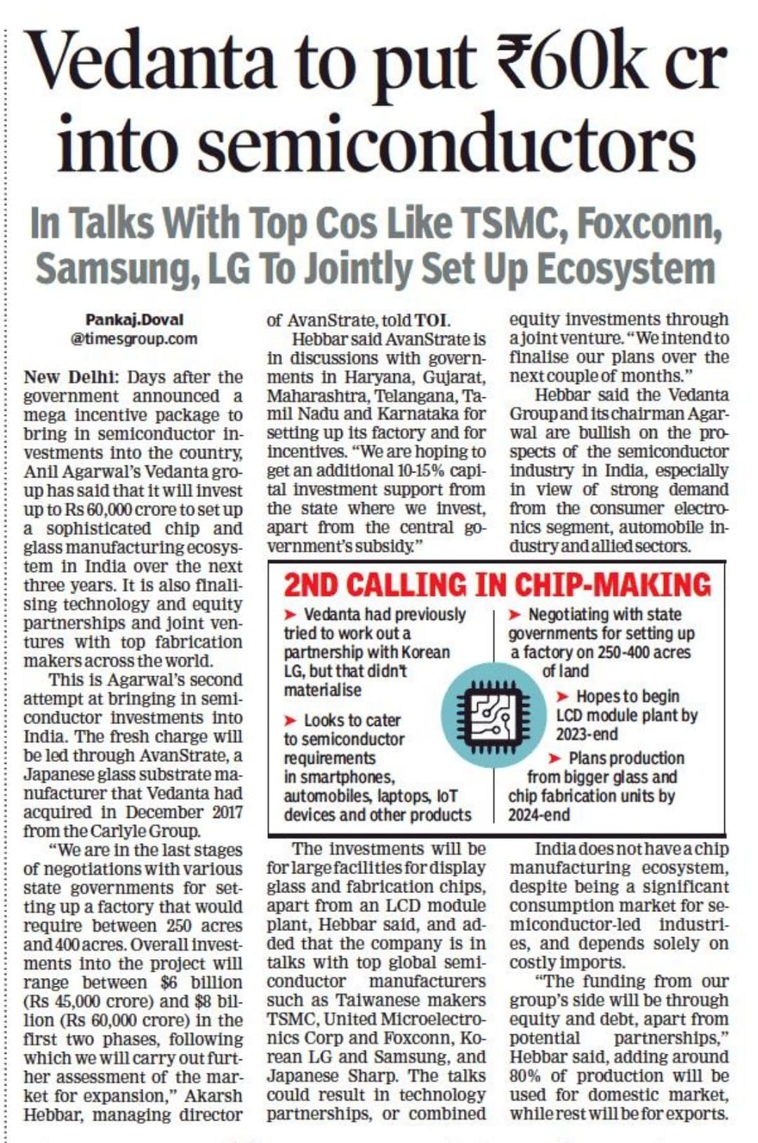
Cabinet decision for $10Bn investment/incentive outlay for developing complete value chain/ecosystem chip/display fabs, packaging, PCBs for Semiconductor sector. As different from other countries offering 50% investments for Setting up chip/display fabs, this claims to be additionally offering a 20 year roadmap (including talent pool proliferation, design-to-startup incentives, et al).
Inviting Domain experts like @rambaranwal and others to lay this out better for us.
(Other undiscovered domain experts at VP, please put your hands up!)
If anyone wants to understand Semiconductor and why TSMC is what it is and why it’s just impossible to have a semiconductor dream without TSMC’s participation. The podcast talks about why in spite of China investing billions and billions of dollars is not able to catch up with TSMC. Hint: it’s not about Money, Honey!!
Podcast also answers why semiconductor is Taiwan.
There is history geography and technology. Do watch, it’s fascinating. I watched it early this year and it was such a Aha moment.
Here is the policy press release.
Some 230000 Cr incentives are being planned for at least 2 semiconductor fabs, 2 display fabs and 20 other items that helps build electronic ecosystem in country.
I think people shall listen to video you uploaded from 7-17 minutes to get an idea of the entire ecosystem. The opportunities lie there. Let me try to break it and elaborate a bit. Semiconductor Fabs:
These are must have components of Electronics Industry. The fabs manufacture Wafers that our IT Minister Mr Ashwani Vaishnav talks about.Yes building latest technology Fabs and competing with Taiwan is not the objective here. Idea is, can we build semiconductor fabs for the most of the items being consumed in India. If I leave the main processor all other semiconductor components come from earlier technologies. We may not have fabs that manufacture Intel processors but we can have fabs that manufacture auto, industrial, Mobile and host of other semiconductors. As for as I know 20 investors have already submitted EOI to Govt. We already have Semiconductor Complex in Chandigarh under ISRO but of old technology. Policy talks about Brown field investment to upgrade that. Semiconductor ATMP/OSAT:
These are not fabs. You get Wafers, test them, package them to build chips. We already have a tiny player in SPEL Semiconductor but that does quite low end job and can grab this opportunity to upgrade. PCB Manufacturers
The packaged part is raw material to our PCB(Printed Circuit Boards). This opens opportunity for PCB Manufacturers. There are many players already doing that. However, they manufacture PCBs and import assembled chips from other places. So another opportunity opens up in PCB Manufacturers. There are many players that can be researched. Discrete Components:
Minister just mentioned its name while explaining the flow but these are not to be ignored. The are passive and active components. This includes companies who design and manufacture SMD Registers, Shunts, Capacitors, Its electrolytes, passive discrete components like DC-DC converters, SMPS etc. We at least know two players like Shivalik Bimetal and PML in passive component space. There are others as well. Design Houses:
Glad to know that there is DLI scheme as well. It would result in new investments towards solution designers who would design products we use or components used in products, say displays. Today assembled flex PCBs are imported from Korea etc though we have some FlexPCB manufacturers already in India. These are imported because of logistical reasons. Its perhaps easy to import an assembled FlexPCB Vs importing 50+ components then assemble here. Once we have these components being manufactured in India it would be easy to develop the ecosystem. Electronic Manufacturing Services:
EMS would get huge boost with semiconductor fabs. All those companies under different sectors who have got PLI have to import semiconductor components until Semiconductors themselves get manufactured in India. Electronic manufacturing is projected to grow at 32.3%, Consumption at 18.4%, and export at 55.3% in next 4 years. BharatFIH DRHP is a good read to understand what this sector alone could enable for India.
Slicon Carbide:
The Semiconductor PLI also includes Silicon Carbide Manufacturing. Why this category is so important? We have Rectifier manufacturers already listed in India. Hind rectifier is one. These rectifiers are used in Power Equipments. Another area that Silicon carbide opens up is IGBTs. The IGBTs would drive EV Vehicle motors when IC engines get replaced by electronic motors. India Electronic Mission is being advised by India Semiconductor Association members and Govt is keenly listening to them. Skilled Resources:
I think there shall be no doubt about it. We started with IT Software as it required minimum investment of a PC/Laptop and real estate. Engineers were plenty and we now know where we are since we started in last 20 years. Then we started VLSI design. Design whole chip was a great achievement 15-20 years back and today we design 50-70% of critical high end products of Global Leaders. We also do end to end validation once assembled chips are back to us. Only link missing is Semiconductor manufacturing, Assembly & Packaging, which this policy ensures. They key is to monitor its progress for next 6 months. If they finalize two fabs and plant starts building it would grow much faster as product demand is already there. RISKS:
The policy timing is coming when chip demand is at high. There are 17 fabs already announced by various players around the world. There is high chance that by the time our fab comes in we may be in oversupply phase and can see bottom of the semiconductor cycle. However, I am sure we can easily consume two fabs capacity in India we are in much better situation than many others.
I have worked for 6 years in a Philips off-shoot, called ASML (Advanced Semicon Material Litho, was the acronym, not used anymore). Majority stake was sold off by Philips about 2 decades ago, when competition from Japanese was bit too much, ironically now only Nikon and Canon survive, but barely, with hardly 3% market each. The company totally dominates its market being a Euro-American high-tech combine, employing the largest number of PhDs in Netherlands (even beating domestic Fortune giants Shell, Unilever, Thales etc.).
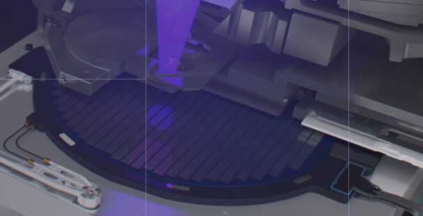
The market it serves is the machine at the heart of a Fab (chip fabrication factory). It is basically a very high-tech printing machine, that etches the circuit pattern on silicon wafers, with laser. This etching is done many times, repeated on same location/die of the silicon, so that as many as 30 layers may be built up on top of one other, and this may take many weeks to do, for manufacture of one single chip/die.
This picture shows, the laser light printing the silicon wafer (the circular disc), each rectangular pattern getting printed is a chip, which will finally get cut out from the silicon disc (wafer).
They sell their machines to Taiwan, Korea, US, Japan and China in that order. Taiwan (TSMC is the biggest giant) does not do much, except run the machines in Fabs and make generic chips for other companies. TSMC gets the best machines and makes the biggest orders, mostly memory chips. Companies in Taiwan manufacture majority of chips.
Next in order comes Samsung etc. plants in Korea, lots of chips, processor, memory, also out-sourced by Apple.
Next by value come Fabs run by Intel, IBM etc, in US.
Japanese just started buying when their own companies started to fail in the smallest (<10 nanometer) printing tech., a few years ago.
Chinese started to buy even later, but have been prevented from buying the top-end machines by Trump’s laws on cutting-edge tech sales, where US patents are involved. They have been trying to reverse engineer the tech at Tsinghua tech institute but have failed for a decade.
From what I hear, Applied Materials is a US company , which is top-supplier of the rest of the chemical processing of the chip circuit pattern, deposit of materials (doping, conducting metals), photo-sensitive coating for printing, polishing etc. So, after each layer of the chip is printed/exposed by laser, it is then developed (like a photo) and chemically treated before next layer is exposed. So, one silicon wafer circulates, up and down the Fab assembly line, multiple times, depending on the complexity of circuit, building up layers.
Each chip/die is finally cut from the circular silicon wafer and packaged in plastic with wires attached as a block we finally see and mounted on a PCB for final assembly in an electronic product/part.
India needs a Fab and it can make the cheaper chips to start with. A Fab needs a clean-room with zero dirt for the critical process machines, high power lasers etc. It takes pure, crystal, silicon wafers and can ship out the printed and developed ones to another factory where the lower-tech process of cutting of individual chips from wafer, their testing and final packaging can be done.
Even lower tech would be just mounting things on PCBs which I guess is already done, more or less in India and is not that specialized.
A Fab is minimum 2-3 billion USD investment, to break even on a commercial scale and even Taiwanese/Koreans take 2-3 years for a greenfield Fab to reach production level quality and throughput. The various equipment vendors and the Fab manufacturing process engineering experts, work together for months, to get the assembly line working. Each machine gets shipped with dozens of engineers and on-site dedicated vendor teams work together with the Fab engineers to keep them running, serviced etc.
Only Tata’s or similar sized business can make this kind of commitment.
The original negative of the photo or the chip design itself, is done by Intel, ARM, Qualcomm, Nvidia, AMD all kinds of chip design companies, where India is already at a decent, advanced stage. Design and Manufacturing have been distanced in the chips supply chain, except when the tech is cutting-edge or specialized and needs to be done in-house. Some like Qualcomm or ARM just sell designs, called Fab-less chip makers. Some are more or less integrated, like Intel, IBM. Some are mostly focused on Fab-only, like TSMC, Global foundry etc. most Taiwan based companies.
Both the intensity and speed of government action on policy front seen recently has been pointing to a resolute intent to sow the seeds of semiconductor manufacturing industry in India. There have been instances in the past when governments have announced schemes to encourage Semicon manufacturing, but that has never taken off. This interesting interview points out why the outcomes could be different this time. Link to the interview below.
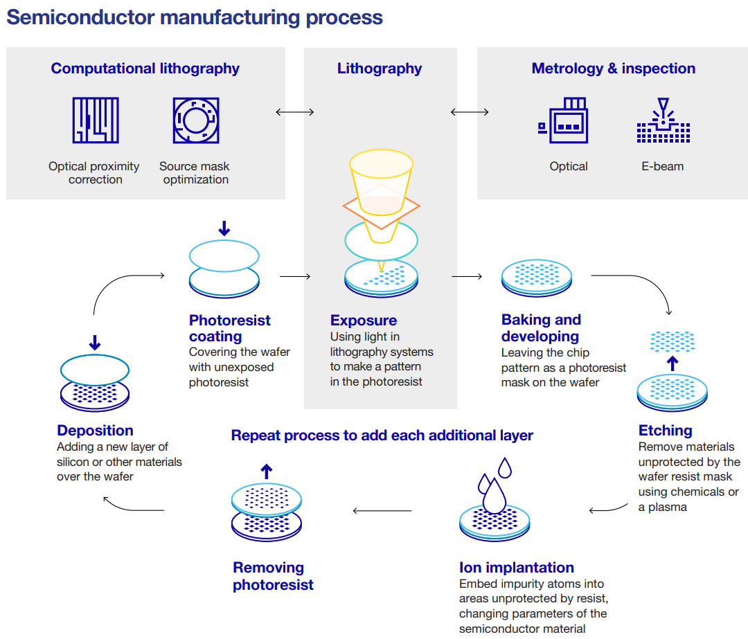
The standard diagram to explain the semi-con chip etc. making process.
My employer only worked in the grey boxes, the most crucial step, that helped make Moore’s law true for the past few decades. Specifically, the science is called metrology, making precise measurements to ensure chip-layers are aligned with nano-meter precision, since each circuit line is typically only few nanometers wide. Laser passes through the “mask” (the chip design template or “photo negative”), and after chemical bath process etc. (kind of “developing the photo”), inspection (of the chip on silicon wafer) is done with electron/optical microscope kind of instruments.
KLA Tencor is a singaporean company also industry leader the grey-boxes on the left and right, except the middle grey-box one the actual “expose” of chip-design on silicon. It may also be doing other steps.
The rest of the mostly chemical processes is not in my domain and where Applied materials, Du Pont etc. comes in.
Apparently it needs lots of water and is polluting hence the industry moved to asia and Taiwan is having a water crisis which partly explains the chip shortages. Also the lasers require very heavy cooling water flow.
Slightly dated news, but significant from that point that the execution machinery is being put in place for government’s plans on promoting Semi-con manufacturing in India. Government has announced the setup of India Semiconductor Mission.
“The India Semiconductor Mission (ISM) is a specialised and independent business division within the Digital India Corporation. It has been set up with the aim to build a vibrant semiconductor and display ecosystem to enable India’s emergence as a global hub for electronics manufacturing and design”