
I have worked for 6 years in a Philips off-shoot, called ASML (Advanced Semicon Material Litho, was the acronym, not used anymore). Majority stake was sold off by Philips about 2 decades ago, when competition from Japanese was bit too much, ironically now only Nikon and Canon survive, but barely, with hardly 3% market each. The company totally dominates its market being a Euro-American high-tech combine, employing the largest number of PhDs in Netherlands (even beating domestic Fortune giants Shell, Unilever, Thales etc.).
The market it serves is the machine at the heart of a Fab (chip fabrication factory). It is basically a very high-tech printing machine, that etches the circuit pattern on silicon wafers, with laser. This etching is done many times, repeated on same location/die of the silicon, so that as many as 30 layers may be built up on top of one other, and this may take many weeks to do, for manufacture of one single chip/die.
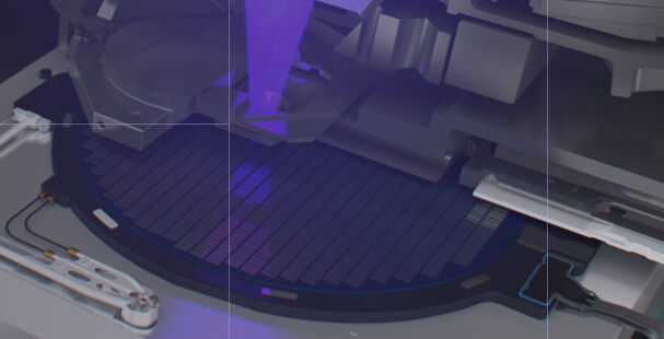
from About ASML | Supplying the semiconductor industry
This picture shows, the laser light printing the silicon wafer (the circular disc), each rectangular pattern getting printed is a chip, which will finally get cut out from the silicon disc (wafer).
They sell their machines to Taiwan, Korea, US, Japan and China in that order. Taiwan (TSMC is the biggest giant) does not do much, except run the machines in Fabs and make generic chips for other companies. TSMC gets the best machines and makes the biggest orders, mostly memory chips. Companies in Taiwan manufacture majority of chips.
Next in order comes Samsung etc. plants in Korea, lots of chips, processor, memory, also out-sourced by Apple.
Next by value come Fabs run by Intel, IBM etc, in US.
Japanese just started buying when their own companies started to fail in the smallest (<10 nanometer) printing tech., a few years ago.
Chinese started to buy even later, but have been prevented from buying the top-end machines by Trump’s laws on cutting-edge tech sales, where US patents are involved. They have been trying to reverse engineer the tech at Tsinghua tech institute but have failed for a decade.
From what I hear, Applied Materials is a US company , which is top-supplier of the rest of the chemical processing of the chip circuit pattern, deposit of materials (doping, conducting metals), photo-sensitive coating for printing, polishing etc. So, after each layer of the chip is printed/exposed by laser, it is then developed (like a photo) and chemically treated before next layer is exposed. So, one silicon wafer circulates, up and down the Fab assembly line, multiple times, depending on the complexity of circuit, building up layers.
Each chip/die is finally cut from the circular silicon wafer and packaged in plastic with wires attached as a block we finally see and mounted on a PCB for final assembly in an electronic product/part.
India needs a Fab and it can make the cheaper chips to start with. A Fab needs a clean-room with zero dirt for the critical process machines, high power lasers etc. It takes pure, crystal, silicon wafers and can ship out the printed and developed ones to another factory where the lower-tech process of cutting of individual chips from wafer, their testing and final packaging can be done.
Even lower tech would be just mounting things on PCBs which I guess is already done, more or less in India and is not that specialized.
A Fab is minimum 2-3 billion USD investment, to break even on a commercial scale and even Taiwanese/Koreans take 2-3 years for a greenfield Fab to reach production level quality and throughput. The various equipment vendors and the Fab manufacturing process engineering experts, work together for months, to get the assembly line working. Each machine gets shipped with dozens of engineers and on-site dedicated vendor teams work together with the Fab engineers to keep them running, serviced etc.
Only Tata’s or similar sized business can make this kind of commitment.
The original negative of the photo or the chip design itself, is done by Intel, ARM, Qualcomm, Nvidia, AMD all kinds of chip design companies, where India is already at a decent, advanced stage. Design and Manufacturing have been distanced in the chips supply chain, except when the tech is cutting-edge or specialized and needs to be done in-house. Some like Qualcomm or ARM just sell designs, called Fab-less chip makers. Some are more or less integrated, like Intel, IBM. Some are mostly focused on Fab-only, like TSMC, Global foundry etc. most Taiwan based companies.