
Apologies for too much tech details!
The standard diagram to explain the semi-con chip etc. making process.
My employer only worked in the grey boxes, the most crucial step, that helped make Moore’s law true for the past few decades. Specifically, the science is called metrology, making precise measurements to ensure chip-layers are aligned with nano-meter precision, since each circuit line is typically only few nanometers wide. Laser passes through the “mask” (the chip design template or “photo negative”), and after chemical bath process etc. (kind of “developing the photo”), inspection (of the chip on silicon wafer) is done with electron/optical microscope kind of instruments.
KLA Tencor is a singaporean company also industry leader the grey-boxes on the left and right, except the middle grey-box one the actual “expose” of chip-design on silicon. It may also be doing other steps.
The rest of the mostly chemical processes is not in my domain and where Applied materials, Du Pont etc. comes in.
Apparently it needs lots of water and is polluting hence the industry moved to asia and Taiwan is having a water crisis which partly explains the chip shortages. Also the lasers require very heavy cooling water flow.
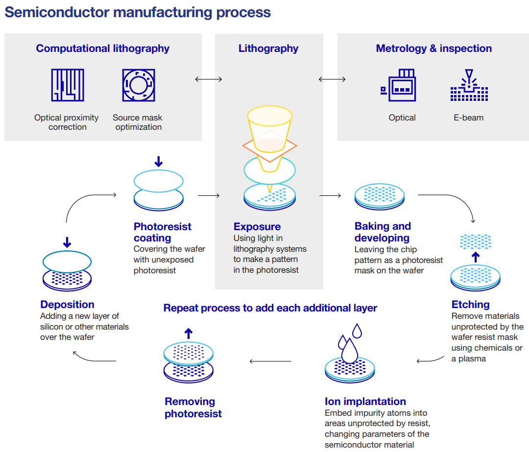
Abbreviations and terms (following clockwise flow of the diagram)
RTP - Rapid thermal processing or the Baking step
Etch - final chip pattern taking shape
CVD - chemical vapor deposition
PVD- physical vapor deposition
CMP - Chemical mechanical planarization (or polishing)
pic taken from ASML AR 2020 (page 12): https://www.asml.com/-/media/asml/files/investors/financial-results/a-results/2020/2020-annual-report-based-on-us-gaap-2er7np.pdf?rev=0c2229f82af04c2985f5ffe4faf9487a